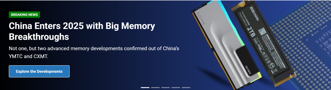
聚焦於半導體行業的知名研究公司TechInsights表示,中國廠商——長江存儲(YMTC)與長鑫存儲(CXMT)均取得了重大技術突破。
在致態最新發布的TiPro9000硬盤中,TechInsights發現了長江存儲的新一代Xtacking4.0 3D NAND芯片。技術分析表明,它的總柵極數高達294層,有着業界最高的TLC位密度!

毫無疑問,這是存儲行業的一大步。TechInsights以“TechInsights Finds YMTC 2yy-layered 3D NAND—the Highest TLC Bit Density Ever!(TechInsights發現了長江存儲2yy層級3D NAND—史上最高的TLC位密度!)”爲題,發佈了專題探討。

目前,這篇內容正位於TechInsights官網首頁的醒目位置,亦有彭博社等多篇報道引用。以下是其原文,並附上我們的翻譯:
“Today, TechInsights found and confirmed China's Yangtze Memory Technology Corporation’s (YMTC) latest and most advanced chip, Xtacking4.x 2yyL 1 Tb 3D TLC NAND. This chip which has the highest number of vertical gates seen in a commercial product to date.”
今天,TechInsights找到並確認了中國長江存儲科技公司 (YMTC) 最新且最先進的芯片:Xtacking4.x技術2yy層級1Tbit 3D TLC NAND。這顆芯片擁有迄今爲止 商業產品中最多的垂直柵極數量。
2yy層級Xtacking4.0芯片,圖自ZOL
“YMTC successfully extended the Xtacking 4.0 memory architecture to 2yy-layered 3D NAND devices despite severe U.S. sanctions against the company. It’s the first 2yy-layered 3D NAND device TechInsights has found on the market.”
儘管美國對該公司實施了嚴厲制裁,長江存儲仍成功地將晶棧Xtacking 4.0存儲架構擴展到2yy層3D NAND器件中。這是TechInsights在市場上發現的第一款2yy層3D NAND產品。
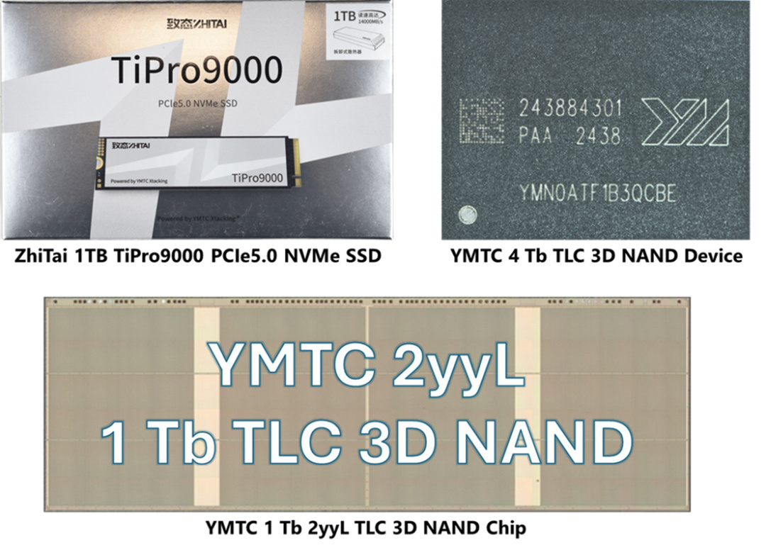
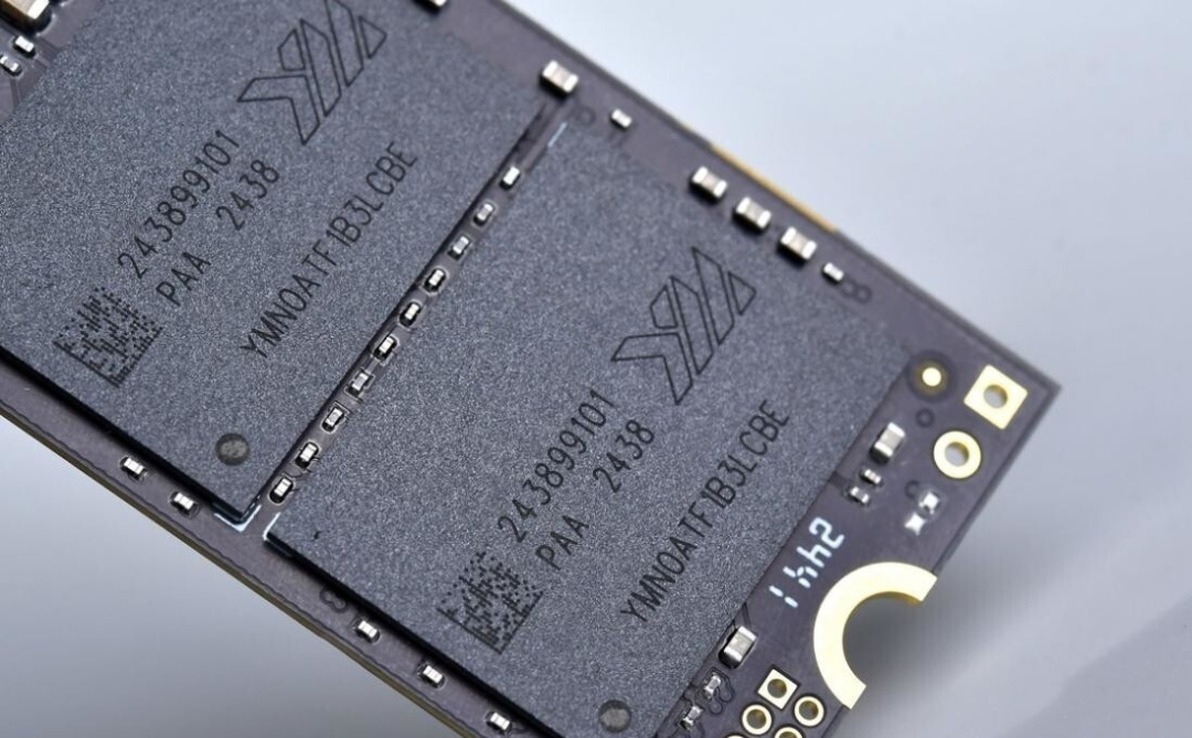
長江存儲2yy層級1Tbit TLC 3D NAND芯片,發現於致態TiPro9000固態硬盤中
“We’re in the process of sourcing 2yy-layer (for example 286L) products fabricated from Samsung and Micron. SK hynix’s 321-layer 4D PUC NAND devices are expected to be on the market in H1 2025 as per TechInsights’3D NAND Technology Roadmap. Yet, the important takeaway is that China’s YMTC has beat the competition to the market with the TLC bit density found in this device.”
我們正在採購由三星和美光製造的2yy層級(如286層)產品。根據TechInsights的3D NAND技術路線圖,SK海力士的321層4D PUC NAND器件預計將在2025上半年上市。然而,重要的地方在於:憑藉其器件的TLC位密度優勢,中國的長江存儲已率先在市場競爭中佔據領先地位。
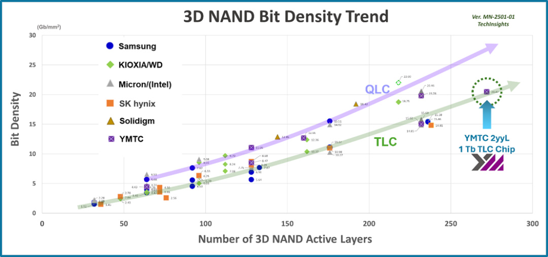
3D NAND的位密度發展趨勢(包括TLC和QLC)
“YMTC’s new Xtacking4.x chip, torn down from the ZhiTai SSD TiPro9000 ZTSS3CB08B34MC, has the YMTC Xtacking4.x structure and design. It consists of 2yy active layers (294L total gates except SGD), 150 gates for the lower deck, and 144 for the upper deck. YMTC maintains its direct bonding (hybrid-bonded) Xtacking structure with two wafers.”
長江存儲的新型Xtacking4.x芯片,是從致態TiPro9000固態硬盤(ZTSS3CB08B34MC)中拆解而來的,擁有長江存儲Xtacking4.x的結構與設計。它由2yy個有源層(除漏極選擇柵極SGD外,總柵極數爲294層)組成,下層擁有150個柵極,而上層則有144個柵極。長江存儲保持了其兩片晶圓直接鍵合(混合鍵合)的Xtacking結構。
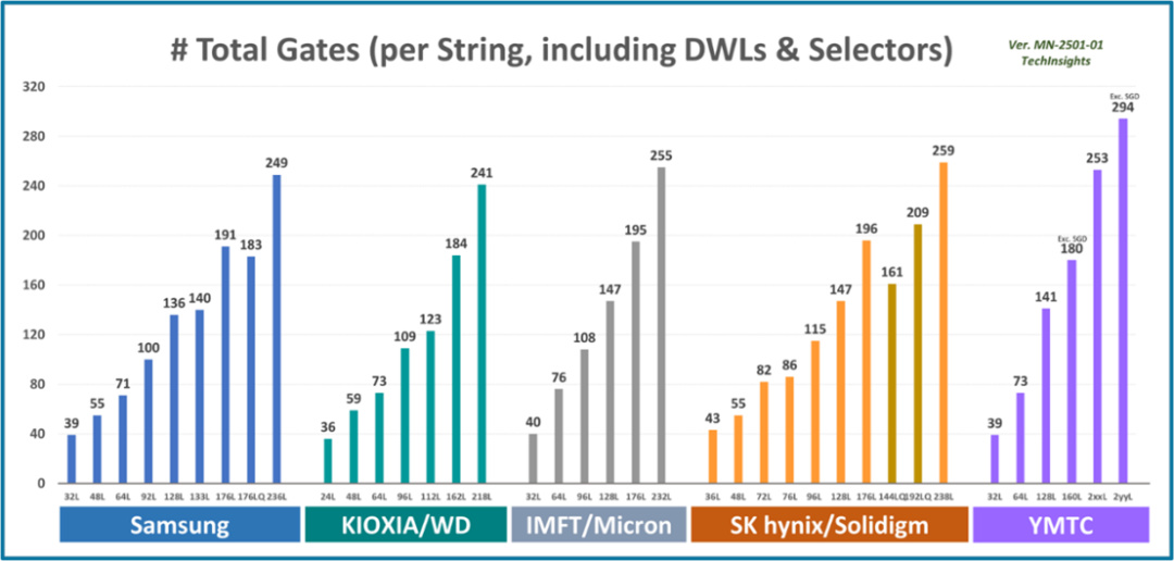
每個3D垂直NAND String中的總柵極數量對比
“The previous Xtacking4.0 160L TLC structure consists of 180 total gates including selectors and dummy gates (except SGD). Vertical channel layouts differ slightly from the previous Xtacking4.0 160L; however, the TLC NAND bit density increases to more than 20 Gb/mm2 for the first time in the industry. We estimate the number of active WLs would be around 270.”
此前的Xtacking4.0 160層TLC結構共計包含180個柵極,其中包括選擇器和虛擬柵極(漏極選擇柵極SGD除外)。2yy層級芯片的垂直溝道佈局與之前的160層Xtacking4.0略有不同;然而,其TLC NAND的位密度增至20Gbit/mm^2以上,這在業界尚屬首次。我們估計,有效字線(WL)的數量約爲270個。
(譯者注:《黑神話·悟空》聯名版TiPlus7100硬盤,便使用了TechInsights所提及的160層Xtacking4.0顆粒——與普通Tiplus7100不同)
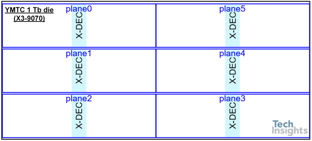
“The YMTC 2yyL 1 Tb 3D NAND die design shows a Center-XDEC design, and the select gate (Poly-Si) on the drain side (SGD) is integrated separately on top of the cell array gates. The backside source connect (BSSC) scheme is still used for the 2yyL structure.”
長江存儲2yy層級1Tbit 3D NAND芯片 採用了中心譯碼器(Center-XDEC)設計,漏極側的選擇柵極(多晶硅,即SGD)被單獨集成在存儲單元陣列的柵極上方。2yy層結構仍然採用了背面源極連接(BSSC)的方案。
(譯者注:“中心譯碼器”有助於減少位線電容,降低tRC延遲,據稱可提升15%~20%性能。長江存儲在Xtacking3.0時代引入了這項設計。)
Xtacking3.0芯片的XDEC示意圖
“When YMTC released Xtacking4.0 devices (for example, 160L) last year,we expected YMTC would combine Xtacking4.0 technology with higher layers such as 2xxL and 2yyL. Because of the U.S. ban, YMTC has been unable to extend 3D NAND fabs and import advanced semiconductor equipment and tools. They needed a detour.
With the new Xtacking4.0 technology, YMTC appears to have found a way to overcome the current bans with this new chip. ”
當長江存儲去年發佈Xtacking4.0器件(如160層)時,我們便預計長江存儲會將Xtacking4.0技術與更高的堆疊層級相結合,例如2xx層與2yy層。由於美國的禁令,長江存儲一直無法擴建3D NAND晶圓廠,也無法進口先進的半導體設備與工具。他們需要繞道而行。
藉助全新的Xtacking4.0技術,長江存儲似乎已經找到了一條道路,通過新的芯片克服現有禁令。
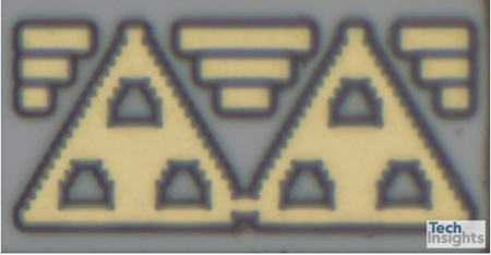
160層Xtacking4.0芯片的特殊“雙峯”符號。TechInsights認爲,這與長江存儲轉向國產設備與材料的戰略密切相關。
“Our technical analysis teams will continue digging into the materials, process integration, and chip design and publishing our findings on the TechInsights Platform as they come available. Please stay tuned.”
我們的技術分析團隊將繼續深入剖析材料、工藝集成及芯片設計細節,並將在TechInsights平臺陸續發佈相關研究成果。敬請關注!
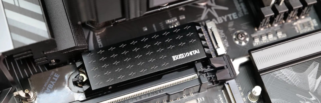
致態TiPro9000硬盤,圖自@噩夢飄雷
(譯者注:我們也將持續注意TechInsights與新一代國產存儲器的消息,同樣敬請關注!)
希望這些內容能幫到你!
更多遊戲資訊請關註:電玩幫遊戲資訊專區
電玩幫圖文攻略 www.vgover.com


